Not All Cleanrooms Are Created Equal: A Deep Dive into Semiconductor Fab Requirements
While the term "cleanroom" is used across many industries, the environment required for semiconductor manufacturing is arguably the most stringently controlled on Earth. As circuit feature sizes shrink to the nanometer scale, a single sub-micron particle or a stray molecule can render a multi-million-dollar wafer useless. This battlefield against contamination requires a facility engineered with uncompromising precision.
Unlike pharmaceutical or medical device cleanrooms, which primarily focus on controlling microbes and viable particles, a semiconductor fab must combat a wider array of invisible threats—from molecular gases and electrostatic discharge to infinitesimal vibrations. This guide explores the five core requirements that define a modern semiconductor cleanroom and explains how they directly impact process yield and device reliability.
Why Semiconductor Cleanrooms Demand Unparalleled Precision
The fundamental challenge in semiconductor manufacturing is defectivity. The "critical dimension" on a modern chip is often smaller than the wavelength of visible light. A single dust particle, measuring 0.5 microns, can be a catastrophic "boulder" on a 5-nanometer circuit path. Yield—the percentage of functional chips per wafer—is directly and inversely proportional to the level of contamination. Therefore, the cleanroom is not just a facility; it is an integral part of the manufacturing process itself.
Core Requirement #1: Extreme Air Cleanliness (ISO 1-5)
The baseline requirement for any cleanroom is particle control, classified by ISO 14644-1. Semiconductor fabrication areas, especially those for photolithography and etching, demand the highest classifications available:
ISO Class 3 (FED-STD 209E Class 1): Typically required for the most critical process areas. This allows for only 10 particles ≥0.1 µm per cubic meter of air.
ISO Class 4-5 (FED-STD 209E Class 10-100): Common for less critical processing and support areas within the main ballroom.
Achieving this requires massive volumes of air passing through ULPA (Ultra-Low Particulate Air) filters, which are 99.9995% efficient at capturing particles down to 0.12 µm.
Core Requirement #2: Airborne Molecular Contamination (AMC) Control
For semiconductors, particles are only half the story. Airborne Molecular Contamination (AMC) refers to harmful gaseous molecules (acids, bases, organics) present in the air, even at parts-per-billion (ppb) concentrations. These molecules can cause:
Unwanted Doping: Changing the electrical properties of silicon.
Corrosion: Damaging metallic interconnects.
Photolithography Hazing: Creating a chemical haze on optical lenses and masks, ruining the patterning process.
Controlling AMCs requires specialized chemical filtration in the HVAC system, using activated carbon or chemisorption media to trap specific molecular threats. Materials used within the cleanroom itself must also be low-outgassing to prevent them from becoming a source of AMC.
Core Requirement #3: Strict Environmental and Utility Control
Process stability is paramount. Even minor fluctuations can alter chemical reaction rates and deposition thicknesses, impacting chip performance.
Temperature Control: Must be maintained within an extremely tight tolerance, often ±0.1°C to ±0.05°C in critical lithography zones.
Humidity Control: Typically held at ±1% to ±2% Relative Humidity (RH) to prevent static buildup and ensure process consistency.
Vibration & Acoustic Control: Lithography and metrology tools are highly sensitive to vibration. The cleanroom slab must be isolated from building vibrations, and individual tools often sit on dedicated vibration isolation platforms. Acoustic levels are also kept low.
Ultra-Pure Water (UPW) and Process Gases: These utilities are the lifeblood of a fab. The cleanroom design must accommodate extensive networks of high-purity piping to deliver these materials to process tools without introducing contamination.
Core Requirement #4: Advanced Airflow and Facility Design
The physical structure of the fab is designed entirely around contamination control.
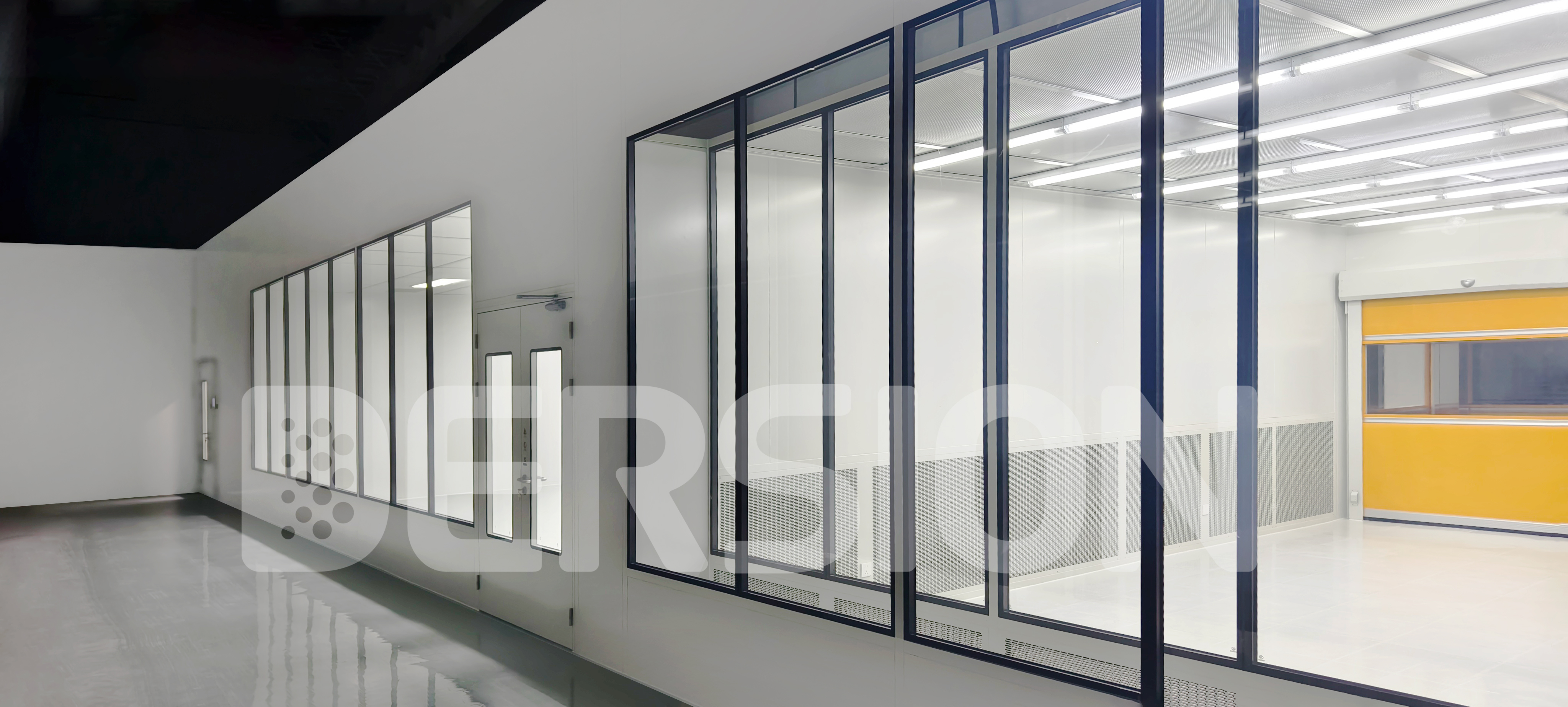
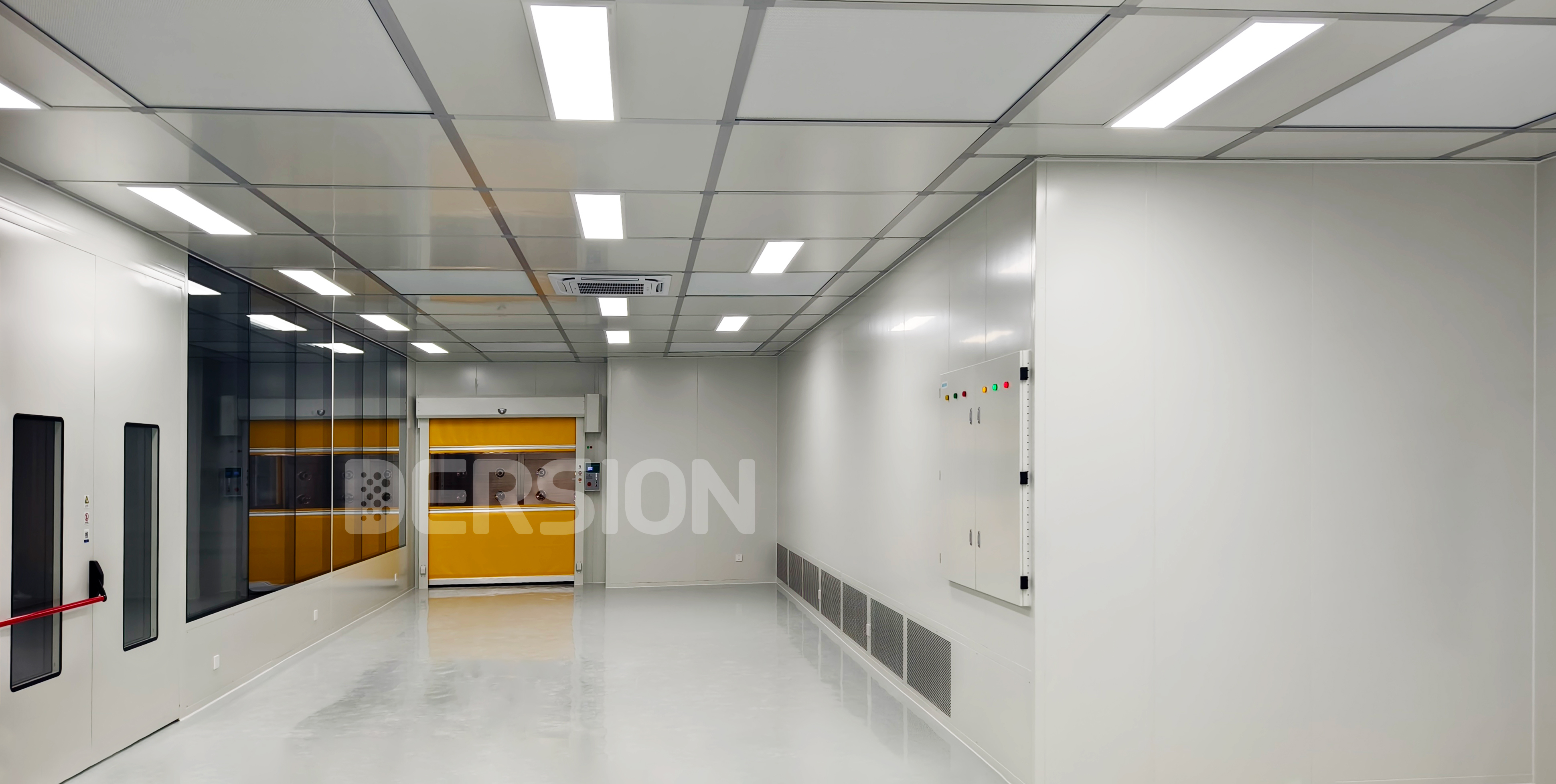
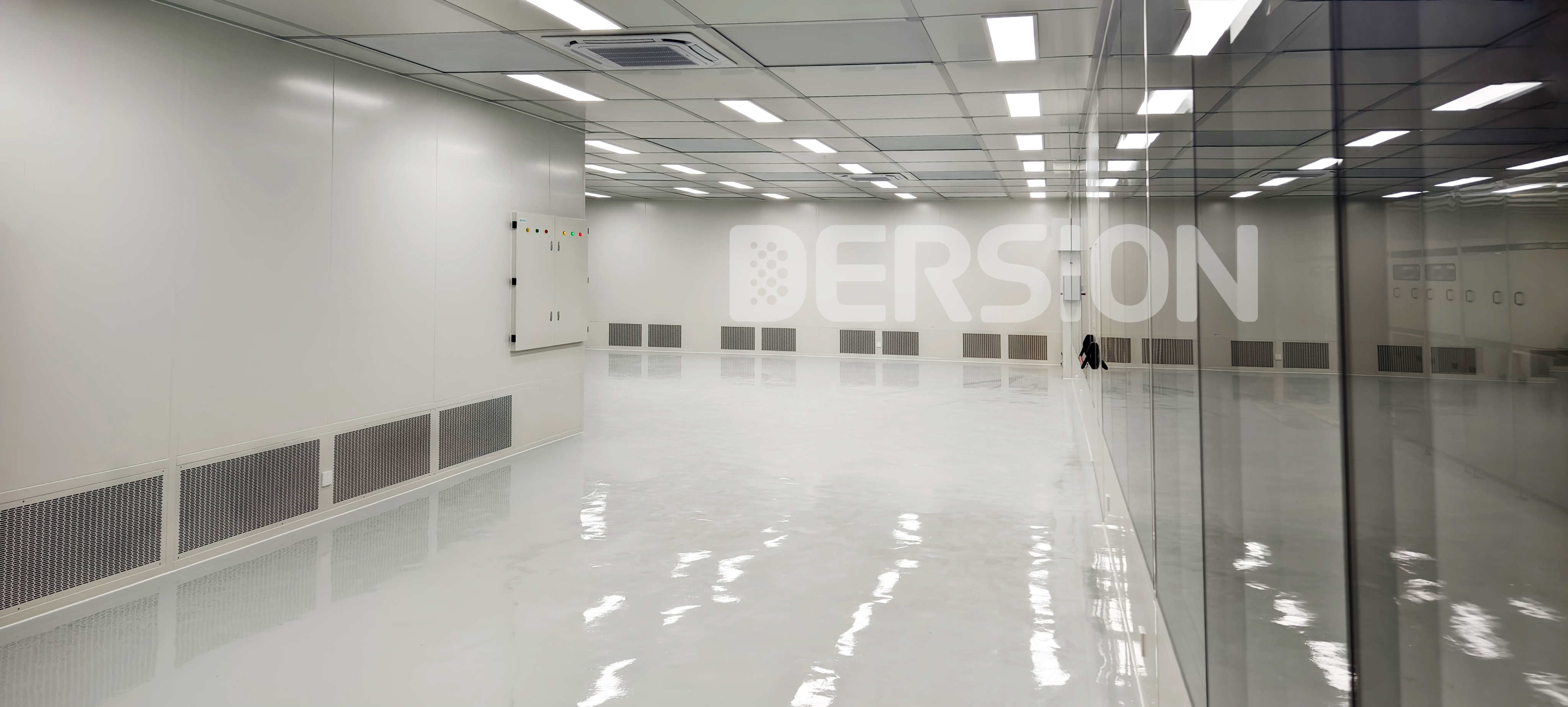
Unidirectional (Laminar) Airflow: The entire ceiling of a semiconductor cleanroom is typically covered in Fan Filter Units (FFUs). These units create a top-to-bottom, piston-like flow of ultra-clean air that continuously pushes particles and contaminants downwards and out of the critical process zone. Air change rates can exceed 600 per hour.
Raised Access Floors: The floor is a perforated grid raised 1-3 meters above the sub-fab. This creates a return air plenum. The unidirectional airflow pushes contaminants through the perforated floor into the sub-fab, where the air is then recirculated back to the FFUs.
Sub-Fab (Utility Level): This area below the cleanroom floor houses pumps, power supplies, gas lines, and other support equipment. This design keeps heat, vibration, and maintenance activities out of the pristine main cleanroom ("ballroom").
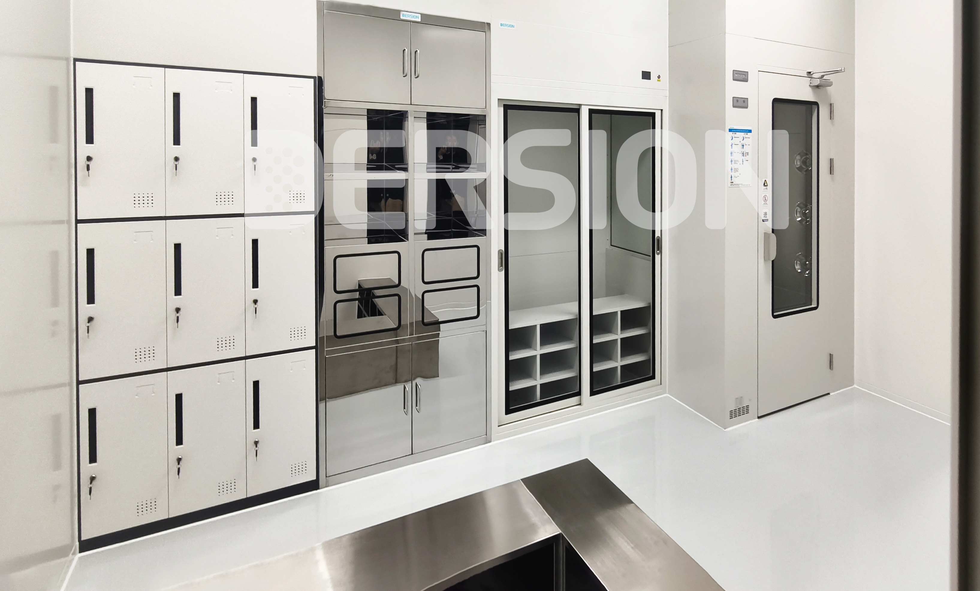
Minienvironments (SMIF/FOUP): To provide even greater control, modern fabs isolate the silicon wafers from the room environment. Wafers travel in sealed pods (SMIF or FOUPs) and are only exposed to filtered air inside the process tool itself, creating an ISO Class 1 environment at the wafer level.

Core Requirement #5: Comprehensive ESD and Static Control
A single Electrostatic Discharge (ESD) event can destroy the microscopic circuitry on a chip. A comprehensive ESD control program is non-negotiable and includes:
- Conductive/Static-Dissipative Flooring.
- Gowning with static-dissipative properties.
- Ionizers installed in FFUs and process tools to neutralize static charges in the air.
- Grounding straps for personnel and equipment.
The System Engineering Approach to Building a Future-Proof Fab
Meeting these five interconnected requirements is a monumental engineering challenge. A change in one parameter (e.g., humidity) can affect another (e.g., static levels). This is where a holistic, system-level approach is critical.
At Dersion, we specialize in the integrated design of large-scale cleanroom facilities. We use tools like Computational Fluid Dynamics (CFD) modeling to optimize airflow patterns, ensuring there are no dead zones where contaminants can accumulate. Our material selection process rigorously vets every component for outgassing and particle-shedding properties. By engineering the structure, HVAC, and control systems as a single, cohesive unit, we deliver facilities that not only meet today's specifications but are also scalable and adaptable for tomorrow's technology nodes.
Planning your next fab or facility upgrade? Contact our semiconductor specialists for a technical consultation to review your specific process requirements.
Post time: Oct-15-2025