
Introduction
In the semiconductor industry, “clean” is a relative term. As nodes shrink to 5nm and below, even a single nanoparticle or a trace of chemical vapor can ruin a silicon wafer worth thousands of dollars. Creating a stable environment for photolithography, etching, and thin-film deposition requires specialized semiconductor cleanroom solutions that go far beyond standard industrial air filtration. Precision infrastructure is not just a support system; it is a critical component of the manufacturing toolset.
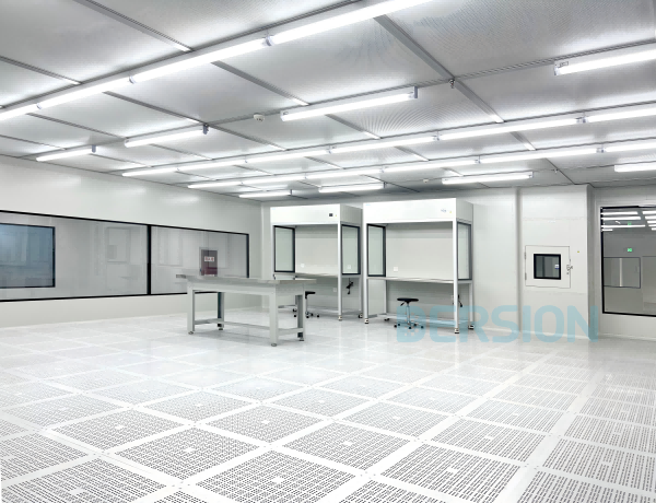
1. Managing Contamination at the Nanoscale
Traditional particulate control is insufficient for leading-edge wafer fabs.
- ISO Class 1 to 5 Precision: While most electronics cleanroom solutions operate at ISO 7 or 8, semiconductor front-end processes often demand ISO Class 5 or higher. Dersion utilizes advanced ULPA (Ultra-Low Penetration Air) filtration systems to capture 99.9995% of contaminants down to 0.1 microns.
- AMC (Airborne Molecular Contamination) Control: Beyond dust, we integrate chemical filters into the Cleanroom HVAC design to eliminate volatile organic compounds (VOCs) and acids that can cause wafer hazing and metal corrosion.
2. Engineering for Tool Stability
Semiconductor lithography equipment is extremely sensitive to external interference.
- Vibration and EMI Management: Dersion’s modular structures can be integrated with independent pedestal systems to decouple mechanical vibrations from sensitive optics. Additionally, we offer specialized panels for Electromagnetic Interference (EMI) shielding, ensuring that high-precision tools operate without signal disruption.
- Modular Agility: The rapid lifecycle of chip technology means fab layouts must change quickly. Dersion’s Modular Cleanroom Solutions provide the flexibility to reconfigure sub-fab areas or expand production bays with minimal downtime.
3. Quality Assurance and Yield Optimization
For a semiconductor facility, the ultimate metric is yield.
- Rigorous Commissioning: Given the stakes, the cleanroom validation IQ OQ PQ process for a fab is exceptionally detailed. Dersion provides the documented performance data needed to prove that the environment remains stable under varying tool loads and occupancy levels.
- Sustainable ROI: By optimizing airflow patterns and utilizing energy-efficient Fan Filter Units (FFUs), we help fab operators reduce Total Cost of Ownership (TCO). This focus on operational efficiency significantly boosts the long-term ROI of the capital investment.
Conclusion
Building a semiconductor facility is a race against time and technology. By leveraging high-performance wafer fab facility designs that prioritize molecular-level purity and structural stability, manufacturers can secure their competitive edge in the global chip market.
External Link
Post time: Sep-17-2026